15
LT3150
3150f
APPLICATIO S I FOR ATIO
U
U
U
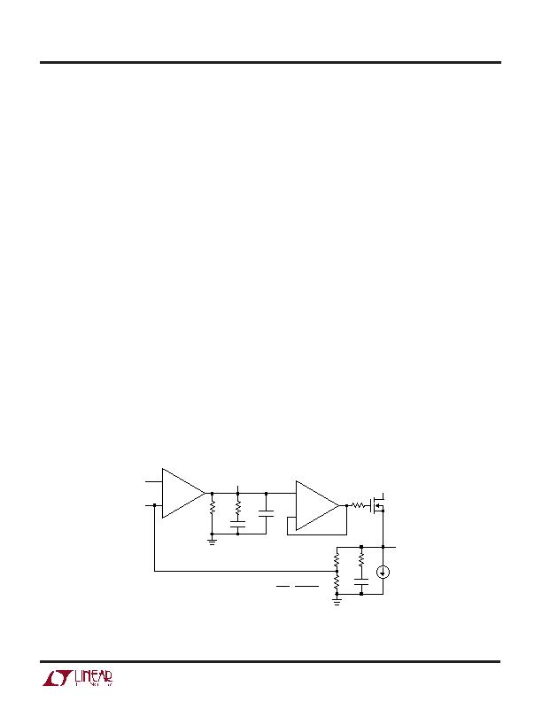
Figure 3. Simplified Block Diagram for Frequency Compensation
+
+
V
REF
FB2
R
O
1M
R1
R
F1
R
ESR
R
F2
R
G
V
IN
V
OUT
I
LOAD
3150 F03
Q1
C1
C2
COMP
g
m1
= 0.015
C
O
V
REF
V
OUT
R
F2
R
F1
+ R
F2
=
Frequency Compensation
Frequency compensation is the most critical step in de-
signing an LT3150 application circuit. Frequency compen-
sation stabilizes the feedback loop under all line, load and
temperature conditions and determines the transient load
step performance.
To start the frequency compensation process, gather the
following application information. Determine the output
voltage, the minimum and maximum output currents, the
transconductance (g
fs
) of the selected MOSFET at the
minimum and maximum output currents and the output
capacitor type (ceramic, tantalum, electrolytic).
Frequency compensation is accomplished with a passive
network tied from the LT3150s COMP pin to ground. The
LT3150 generally employs a Type-2 frequency compensa-
tion method. The
Type-2
method uses two poles and one
zero. The output capacitor type determines how the zero
in the feedback loop is set. Ceramic capacitors typically
have very low ESR (equivalent series resistance) and
therefore the COMP pin network sets the
zero
location.
Tantalum and electrolytic capacitors typically have suffi-
cient ESR such that the
zero
formed by the ESR and the
capacitance value is used. Using tantalum or electrolytic
capacitors in LT3150 applications is somewhat more
challenging because the user must choose capacitors with
the proper ESR plus capacitance value to place the zero at
the correct spot in the frequency response.
Refer to the simplified LT3150 block diagram shown in
Figure 3 during the frequency compensation discussion
that follows.
Figure 4 illustrates the typical bode plot and the pole/zero
locations with the use of low ESR ceramic output
capacitors.
Figure 5 illustrates the typical bode plot and the pole/zero
locations with the use of tantalum or electrolytic output
capacitors.
In both output capacitor cases, the location of the first
pole, P1, is set by the error amplifier COMP pins open-
loop output impedance, R
O
, and compensation capacitor,
C1. The low frequency gain is set by g
m1
" R
O
" (V
REF
/V
OUT
)
In the case of low ESR ceramic capacitors, R1 in series
with C1 in the COMP pin network sets the zero, Z1. With
tantalum or electrolytic capacitors, the ESR in series with
the output capacitor C
O
sets Z1. Z1s location establishes
the mid-band gain or
shelf
gain. For a given value of
output capacitance, the
shelf
gain determines the
regulators transient response to an output load step,
especially the output voltages peak overshoot and under-
shoot. For a given output load current change, a corre-
sponding delta in the MOSFETs V
GS
occurs. This V
GS
divided by the
shelf gain
sets how much the FB2 must
change and thus, results in output voltage perturbation.
Higher
shelf
gain results in lower transient response
peak deviations. Higher shelf gain also translates to a
发布紧急采购,3分钟左右您将得到回复。
相关PDF资料
LT3500HMSE#TRPBF
IC REG DL BUCK/LINEAR 16-MSOP
LT3507HUHF#TRPBF
IC REG QD BUCK/LINEAR 38-QFN
LT3570IFE#TRPBF
IC REG BUCK/BST/LINEAR 20TSSOP
LT3645HMSE#TRPBF
IC REG DL BUCK/LINEAR 12-MSOP
LT3694IFE-1#TRPBF
IC REG TRPL BUCK/LINEAR 20TSSOP
LT4220IGN#TR
IC CTLR HOTSWAP DUAL 16-SSOP
LT4250LCN8
IC CONTRLR HOT SWAP NEG 48V 8DIP
LT4254CGN
IC CTRLR HOTSWAP POSVOLT 16SSOP
相关代理商/技术参数
LT317
制造商:LINER 制造商全称:Linear Technology 功能描述:Positive Adjustable Regulator
LT317A
制造商:LINER 制造商全称:Linear Technology 功能描述:Positive Adjustable Regulator
LT317AH
制造商:LINER 制造商全称:Linear Technology 功能描述:Positive Adjustable Regulator
LT317AHV
制造商:LINER 制造商全称:Linear Technology 功能描述:High Voltage Positive Adjustable Regulators
LT317AHVH
制造商:Linear Technology 功能描述:LDO Regulator Pos 1.5A 3-Pin TO-39
LT317AHVK
制造商:LINER 制造商全称:Linear Technology 功能描述:High Voltage Positive Adjustable Regulators
LT317AK
制造商:LINER 制造商全称:Linear Technology 功能描述:Positive Adjustable Regulator
LT317AT
功能描述:IC REG LDO ADJ 1.5A TO220-3 RoHS:否 类别:集成电路 (IC) >> PMIC - 稳压器 - 线性 系列:- 产品培训模块:More Information on LDOs 标准包装:50 系列:- 稳压器拓扑结构:正,固定式 输出电压:3.3V 输入电压:最高 15V 电压 - 压降(标准):1.1V @ 800mA 稳压器数量:1 电流 - 输出:800mA 电流 - 限制(最小):800mA 工作温度:0°C ~ 125°C 安装类型:表面贴装 封装/外壳:TO-263-4,D²Pak(3 引线+接片),TO-263AA 供应商设备封装:D2PAK-3 包装:管件